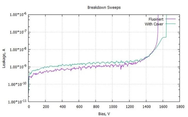
Traditional test systems used for WLR, PCM, and Die-Sort do not have the measurement dynamic range or resolution to meet the new efficiency requirements (higher voltage, lower leakage current, lower on-resistance), or they require time-consuming manual reconfiguration to switch between low- and high-voltage tests. To meet your fab’s productivity goals, you can no longer afford to manually switch between two separate test systems for low voltage and high voltage testing. Only Keithley can perform fully automatic wafer-level tests up to 3kV in a single probe touchdown.
Move from high voltage to low voltage without changing test set up.
Perform all high- and low-voltage tests in a single pass without changing equipment or test setup. Get full 3kV sourcing capability combined with sub-pA measurement resolution, which eliminates the need to re-configure the test setup or use two separate test systems when moving from high voltage to low voltage breakdown tests. Minimize connectivity issues due to manual cabling and probing. Reduce false failures by ensuring high quality measurements. Safely rely on test results to adjust manufacturing process parameters to maximize yields.
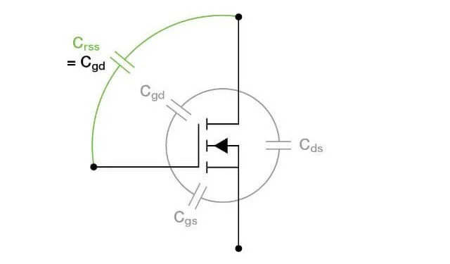
Measure capacitance without manual reconfiguration
Automate all Capacitance tests, including complex 3-terminal measurements. Fully automate
2- or 3-terminal transistor capacitance measurements to quickly evaluate switching characteristics such as speed, energy, and charge with Keithley’s high voltage switching matrix.
Minimize test times, maximize test throughput and reduce cost of test with Keithley’s
Test Script Processing (TSP) technology and virtual backplane (TSP-Link) that enables
high-speed triggering, timing, and synchronization between all elements of the system.
High Voltage Wafer Testing in a Production Environment Achieving Maximum Parametric Test Throughput
Application Note Application Note
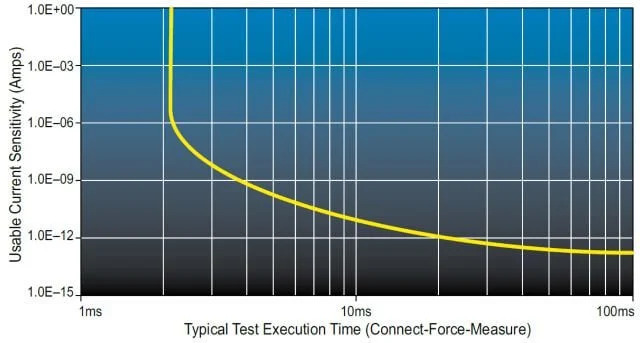
This application note explores several measurement techniques and approaches This application note addresses recent developments in system
that enable automated HV wafer level characterization on multiple pins without test speed optimization and offers general guidelines for test
sacrificing low voltage performance or throughput, as well as share results and speed optimization at both the system and specific test algorithm
experiences in the emerging field of HV wafer-level testing. level.
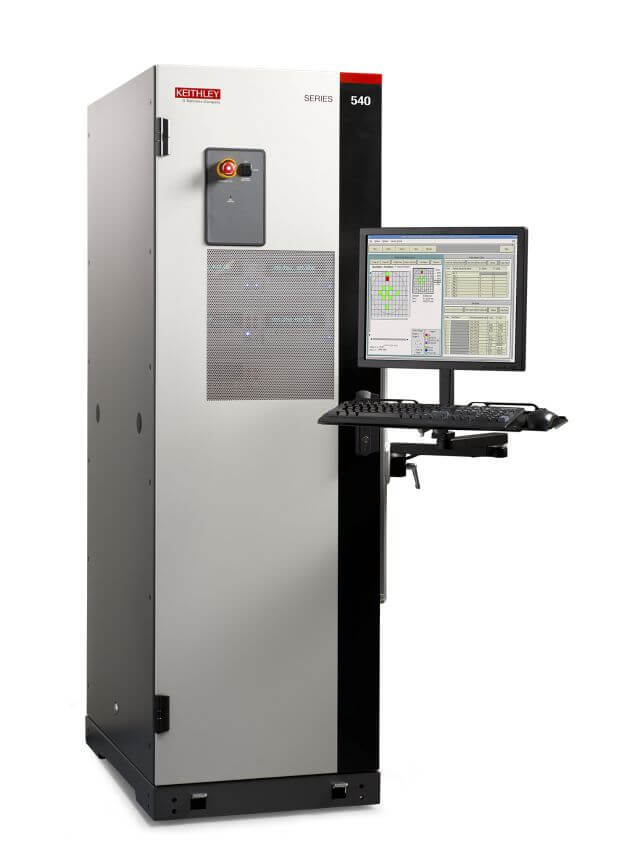
Complete, single-pass parametric testing up to 3 kV Test With More Accuracy and Fidelity
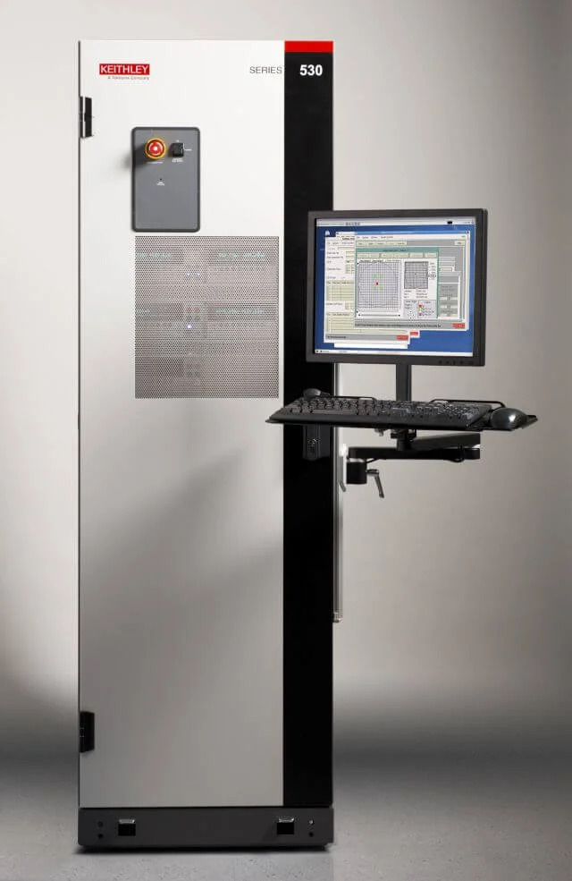
The 540 Parametric Test System is a fully-automated, 48 pin parametric test S530 Parametric Test Systems are designed for production and lab
system for wafer-level testing of power semiconductor devices and structures environments that must handle a broad range of devices and
up to 3kV. technologies, offering industry-leading test plan flexibility, automation,
probe station integration, and test data management capabilities
-Optimized for use with the latest compound power semiconductor -Readily adaptable to new devices and test requirements
materials including silicon carbide (SiC) and gallium nitride (GaN) -Fast, flexible, interactive test plan development
-Fully integrated to perform all high voltage, low voltage, and -Compatible with popular fully automatic probe stations
capacitance tests in a single probe touch-down. -Options for 1kV, C-V, pulse generation, frequency
measurements, and low-voltage measurements
Facing challenges in other power applications?
Characterization of Power Characterization and Troubleshooting Maximizing Battery Life of IoT Devices
Semiconductor Devices of Power Conversion Designs
 KALİBRASYON LABORATUVARI
 Fast automation