Get Your Power Semiconductor Devices to Market Faster
Demanding applications in automotive electrification and RF communications require wide bandgap semiconductor technology such as SiC and GaN along with the continued use of traditional silicon. SiC and GaN offer higher voltage operating frequencies, and higher temperatures with lower power loss compared to Si. Understanding the electrical performance of SiC and GaN will help enable a strong value proposition for their use in many emerging power applications. Get to market faster for your power semiconductor devices while minimizing device failures in the field.
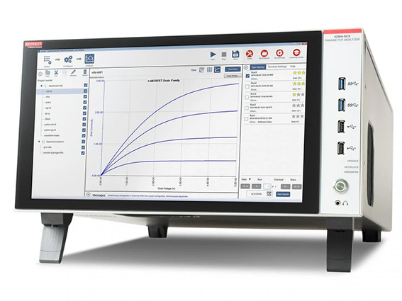
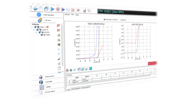
I-V Characterization Measurements for Wide Bandgap Semiconductors
 I-V Characterization
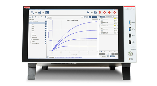
I-V Characterization is a fundamental method of understanding the current versus
voltage relationship of silicon, silicon carbide, and gallium nitride’s fundamental
properties. Using instruments like SMUs or parameter analyzers and appropriate
software, an I-V graphical curve is generated that is used to show the relationship
between the current flowing through an electronic device or circuit and the applied
voltage across its terminals. The most common set of I-V curves is the family of
curves.
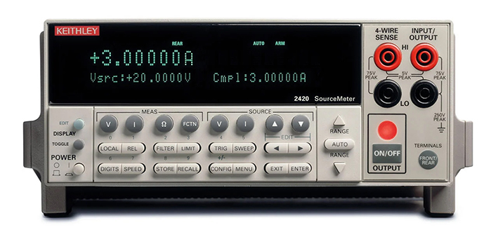
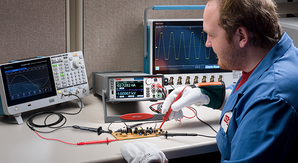
DC I-V Characterization of MOSFET Devices Using KickStart Software
I-V Characterization
 Test Across Wide Power Envelopes
Characterizing SiC or GaN wafer- and packaged-part level devices for electrical
performance requires learning new techniques, such as utilizing higher power
instruments, dealing with the challenges of probing and making low level
measurements such as picoamp levels of leakage current in the presence of high
breakdown voltages. With wide bandgap semiconductors, it’s more common to be
sourcing voltages as high as 3000 V and currents up to 100 A. Just as important is
optimizing the testing system to reduce the amount of time it takes to change setups
for making ON-state, OFF-state, and capacitance measurements.
Solving Connection Challenges in On-Wafer Power Semiconductor Device Test Application Note
 Breakdown Testing of Power Semi
Devices
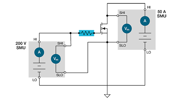
A device’s OFF-state breakdown voltage determines the maximum voltage that can
be applied to it. The primary withstand voltage of interest to power management
product designers is the breakdown voltage between drain and source of a MOSFET
or between the collector and emitter of an IGBT. For a MOSFET, the gate can be either
shorted or forced into a “hard” OFF state, such as by applying a negative voltage to
an n-type device or a positive voltage to a p-type device. This is a very simple test
that can be performed using one or two source measure unit (SMU) instruments.
Breakdown and Leakage Current Measurements on High Voltage Semiconductor
Devices
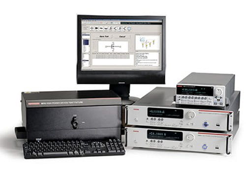
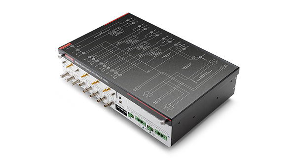 Connecting Instruments to Prober and
Test Fixtures
Connecting high power instruments to probe stations and test fixtures can be a
complicated task. Improper connections can often lead to measurement errors. The
8020 High Power Interface Panel provides a highly accurate, flexible, and easy to use
interface between Keithley SMUs and a variety of semiconductor probe stations or
custom test fixtures. The interface panel has six measurement pathways
accommodating 3 kV, 200 V, and 100 A measurements. You can configure five of the
pathways with a variety of output connector types to match your probe station. You
can configure four pathways with the optional bias tees. This provides high-voltage
C-V measurements on up to four pins of the device under test.
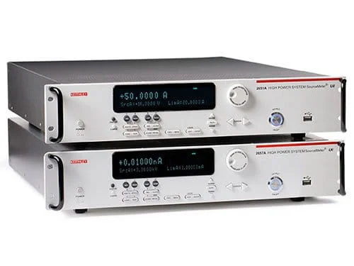
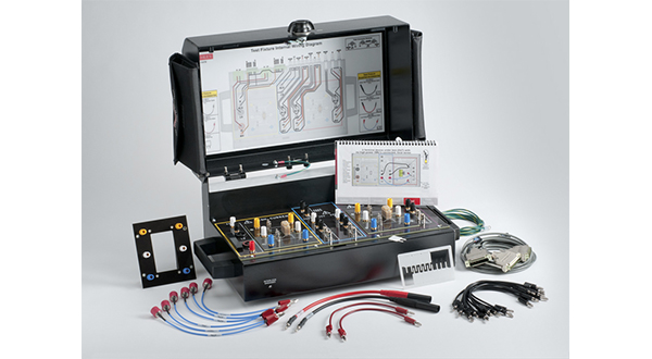 Safety First When Conducting High Power
Tests
Safety should always be at the top of your mind when conducting high power tests
on wide bandgap semiconductors. Designing a safe and compliant test fixture for
the lab is not trivial. The 8010 High Power Device Test Fixture provides a safe, low
-noise, complete environment for testing a variety of packaged device types up to
3000 V and 100 A. The replaceable socket module test boards allow for a variety of
package types, including user-supplied socket types.
 Automate Power Sequencing for I-V
Characterization
Save the trouble of programming your test with Keithley’s Automated
Characterization Suite (ACS) Software. ACS is a flexible, interactive software
test environment designed for device characterization, parametric test, reliability
test, and even simple functional tests. ACS supports a wide array of Keithley
instrumentation and systems, hardware configurations, and test settings. With
ACS, users are able to configure their instrumentation using the automated
hardware management tool and perform tests quickly without the need for
programming knowledge.
Power Sequence for GaN HEMT Characterization
Products
 KALİBRASYON LABORATUVARI